Gerber'd quasi-Yagi — SMA on PCB (rear tab or emitter) / pigtail (stand-mount)
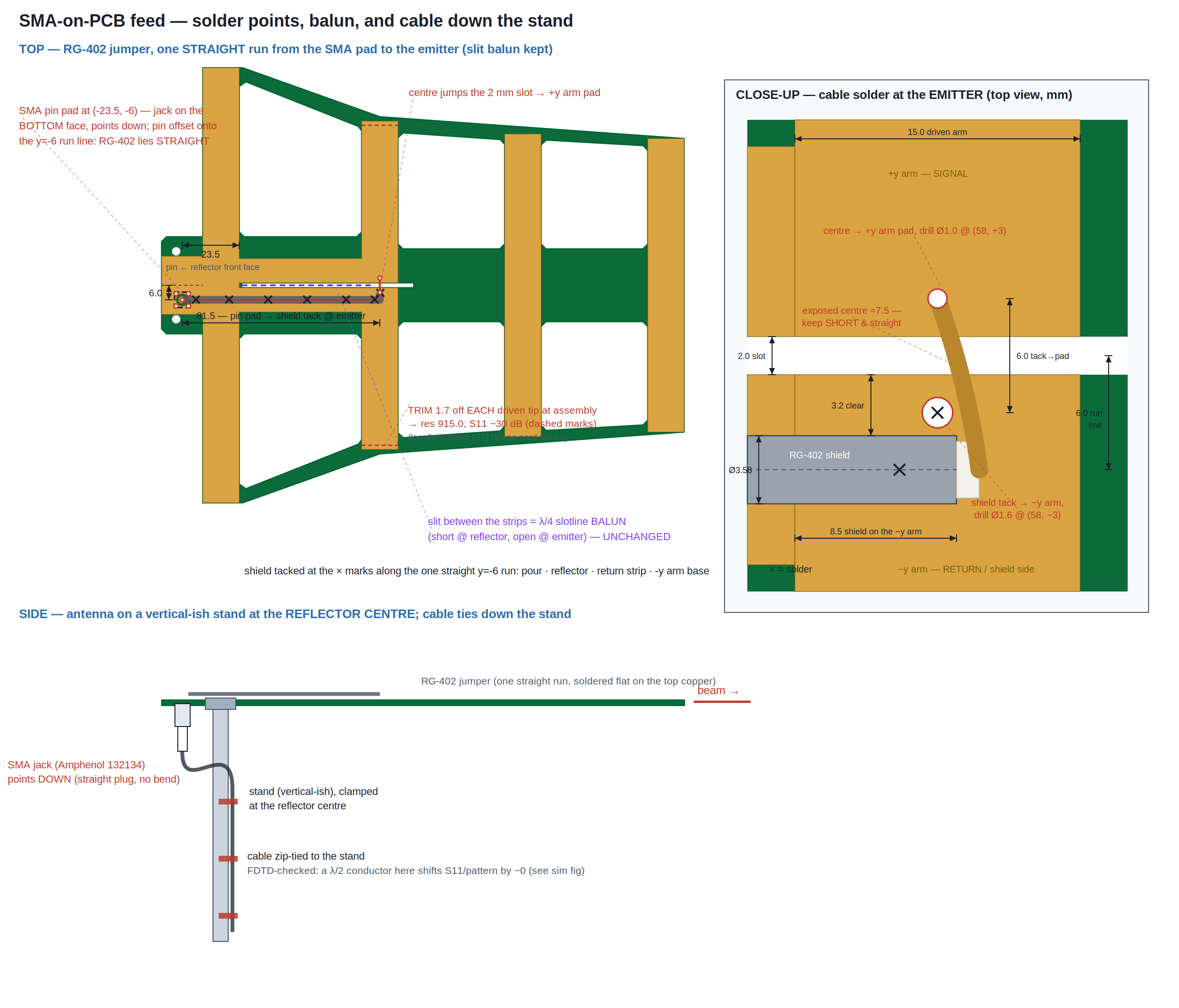
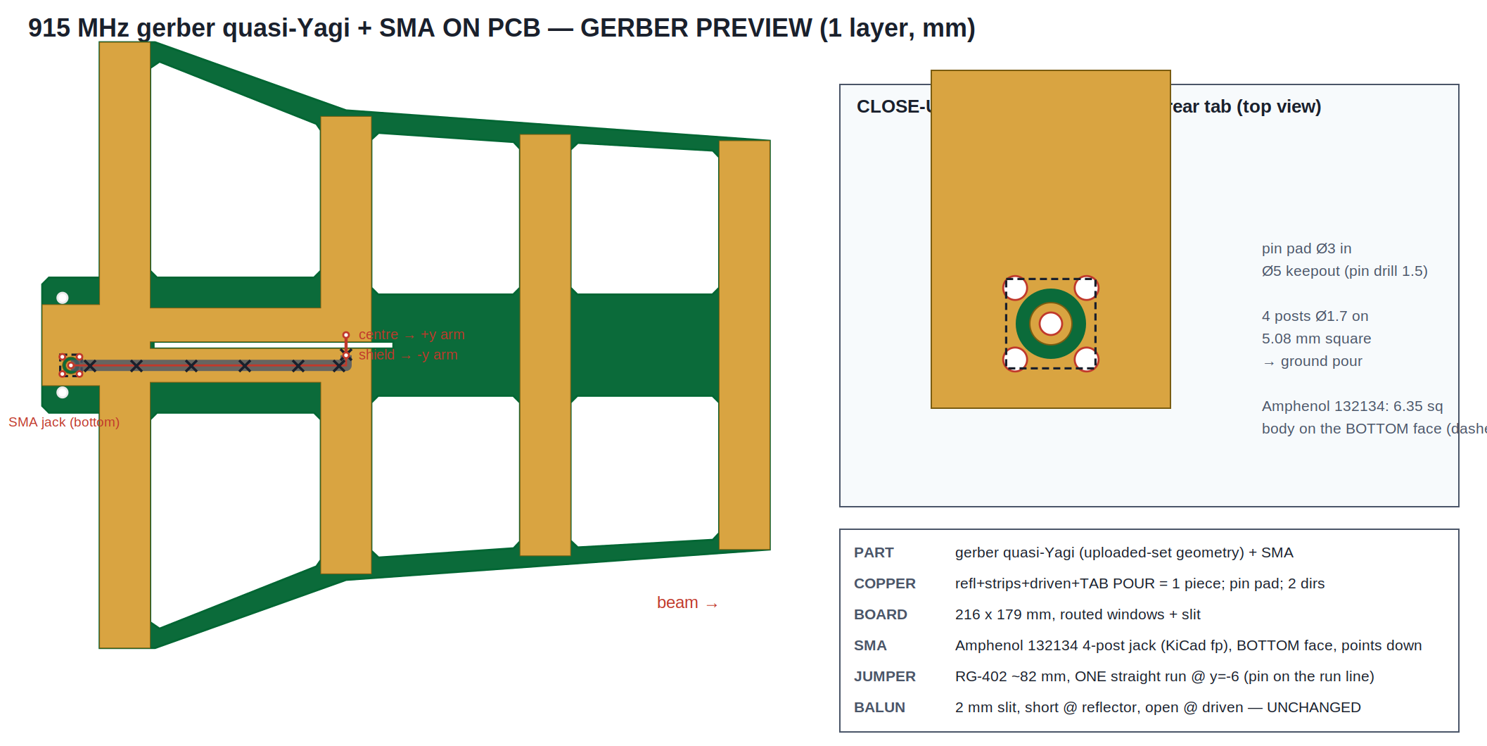
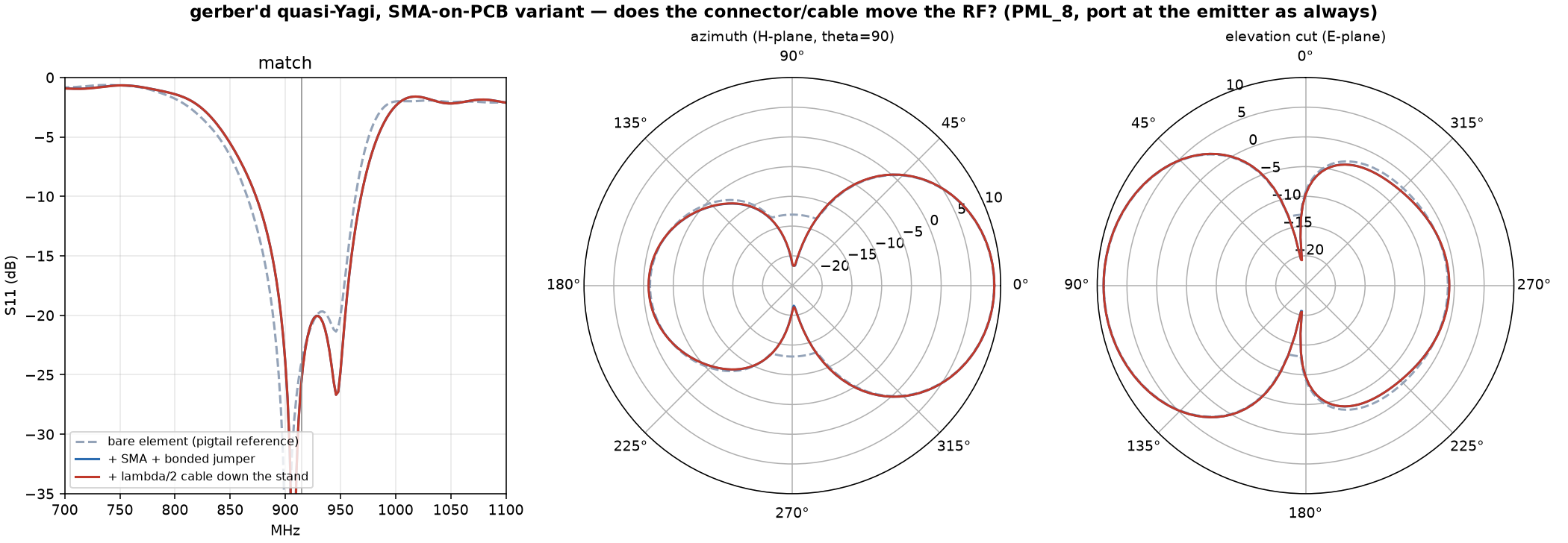
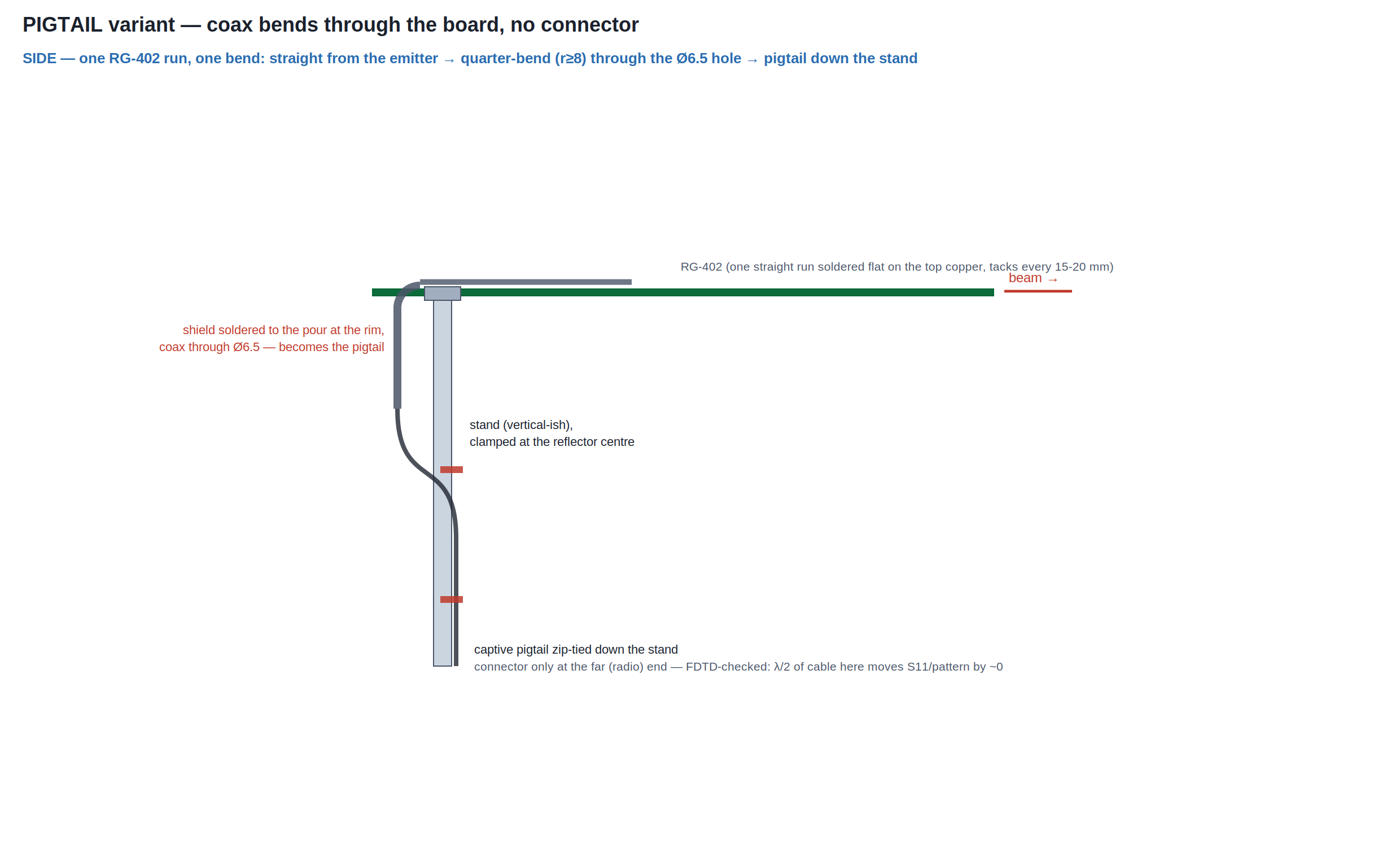
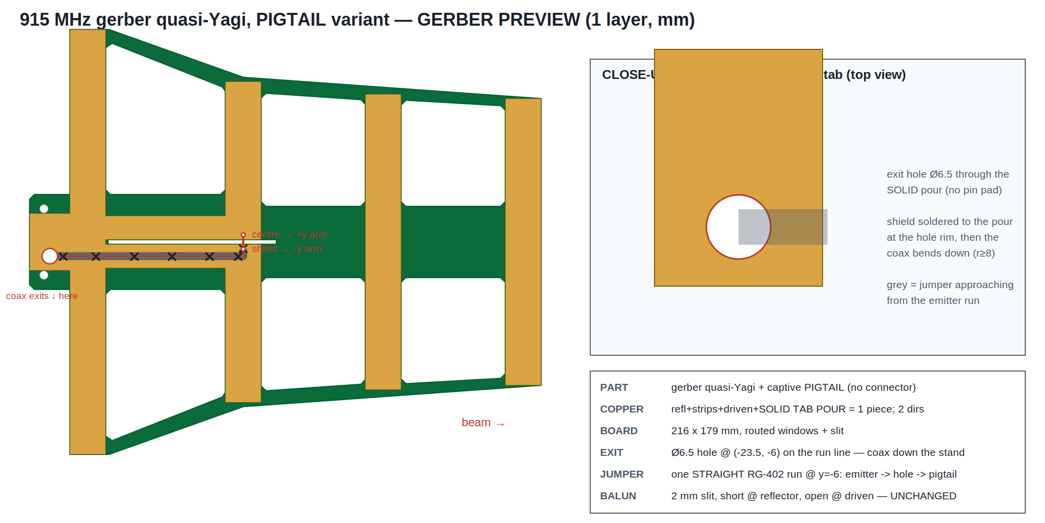
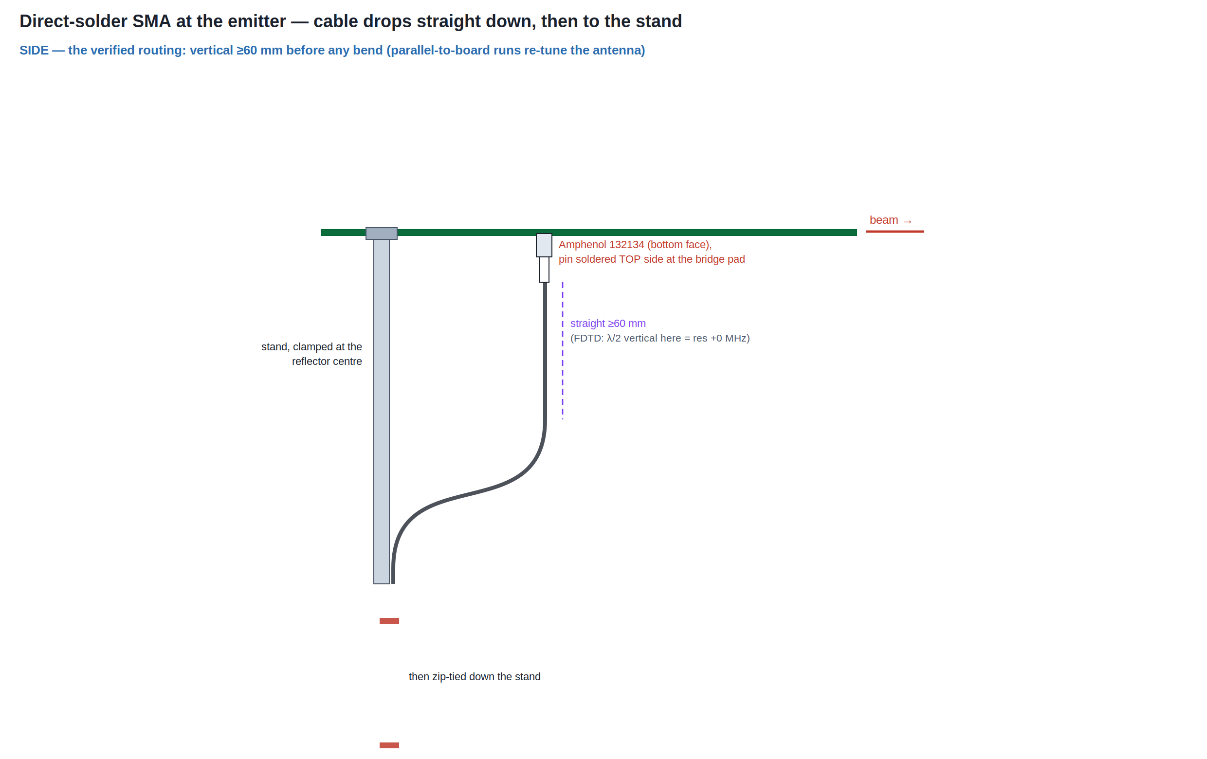
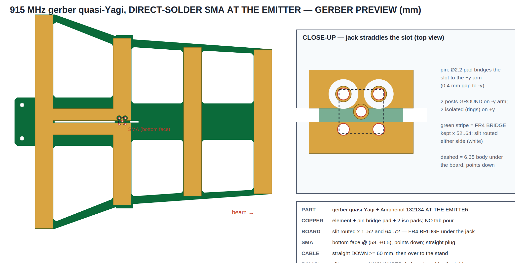
8.9 dBi · F/B 9.8 dB · S11 -26.1 dB @915 (res 908 MHz wide-port model; AS-BUILT the localized-drive model puts the untrimmed board at ~892 MHz — apply the 1.7 mm/tip trim in the tables below to centre 915.0 at S11 -30.5 dB) · SMA ON THE PCB — REAL LIBRARY PART, not invented: Amphenol 132134 4-post flange jack (KiCad packages3D STEP, measured 6.35 mm sq × 9.55; official KiCad footprint drills: pin 1.5, posts 1.7 on a 5.08 mm square) on the BOTTOM of the rear FR4 tab at (−23.5, −6) — deliberately OFF the tab centre, the pin sits dead in line with the y=−6 return-strip run so the stiff jumper needs ZERO on-board bends — pointing DOWN along the vertical-ish stand that clamps the reflector centre, so the cable takes a straight plug and zip-ties down the stand, exiting in the pattern's rear null · RG-402 semi-rigid jumper (0.141", Ø3.58, ~82 mm — min bend r ~8 mm, which is exactly why the connector moved to the run line instead of the cable jogging to it) flat on the top face in ONE STRAIGHT RUN: centre → Ø3 pin pad (Ø5 keepout), shield seam-tacked along the tab GROUND POUR (bonded to the reflector at x=−15) → reflector → return strip → −y arm base; at the emitter the centre jumps the 2 mm slot to the +y arm pad — FEED POINT AND 58 mm SLIT BALUN UNCHANGED from the gerber_yagi element · FDTD A/B (PML_8, port at the emitter as always): bare 8.87 dBi / F/B 10.0 / res 902 → +SMA hardware 8.94 / 9.8 / 908 → +λ/2 CABLE down the stand 8.93 / 9.8 / 908 — the connector nudges resonance toward 915 and the cable then changes nothing (ΔS11 0.1 dB): the offset rear-tab position is just as field-quiet as the old centred one and the design stays CABLE-INDEPENDENT (the common-mode check the slit balun must pass) · modelled: real-size body + post blades + jumper EXTERIOR as bonded metal (the jumper interior is 50 Ω coax by construction); worst-case cable = bare λ/2 rod off the connector · MUR sanity A/B agrees · tab strain holes (−26, ±14) kept for a backup zip-tie · single element for a stand mount; the Σ/Δ finder pair can adopt the same rear-tab SMA per board · Gerber set parses clean (gerbonara) · 3D: STEP assembly (cadquery/OpenCASCADE — board, copper, the KiCad library connector, RG-402 swept along the route, now a single straight segment; CST/Onshape-ready) + interactive rotating 3D (three.js, real tessellated connector) with the stand/cable context · PIGTAIL ALTERNATE BUILD (second Gerber set, no board connector): the same RG-402 run, instead of landing on a pin pad, BENDS DOWN (r≥8) THROUGH A Ø6.5 EXIT HOLE at the pin-axis spot (−23.5, −6) — on the run line, so this quarter-bend is the cable's ONLY bend — and continues as a CAPTIVE pigtail down the stand; the tab pour is SOLID and the shield is soldered all around the hole rim (ground bond + strain relief); connector only at the far radio end · FDTD (PML_8): pigtail 8.95 dBi / F/B 9.8 / res 908 / S11 -26.4 dB @915 vs bare 8.87 / 10.0 / 902 — same behaviour as the SMA build (the exit is the same field-quiet spot); trade-off: ~0.05–0.1 dB less loss and no connector cost/height, but re-cabling means desoldering · DIRECT-SOLDER SMA AT THE EMITTER (third build, third Gerber set — no jumper at all): the same Amphenol 132134 vertical jack on the BOTTOM face right at the feed, offset to (58, +0.5) so the Ø2.2 pin pad bridges the slot into the +y arm (0.4 mm fab-safe gap), the two −y posts ground on the −y arm (= the shield bond), the two +y posts sit on ISOLATED ring pads; an FR4 BRIDGE stays in the routed slit (x 52–64) and the outline bumps to ±72.5 over the driven element · footprint survey (KiCad Connector_Coaxial, all families): every THT SMA uses the same pin+4-post ±2.54 square and every edge/SMT family is GSG — no standard layout suits a coplanar 2 mm slot, so the offset recipe is the practical optimum · the jack body under the feed is NOT free (unlike the field-quiet rear tab): it detunes ~+30 MHz and raises the feed R to ~61 Ω → driven RETUNED l_drv 135.4→140 (swept 139–145, MUR + PML; tuned on S11@915 — the S11 curve is double-dipped so the argmin 'resonance' readout hops between dips) · FDTD (PML_8) @915: jack 8.85 dBi / F/B 9.8 / S11 -17.9 dB; +λ/2 cable STRAIGHT DOWN 8.76 / 9.6 / -18.5 dB (VSWR ≈ 1.27, Zin 61−7j — matched a shade shallower than the rear builds' −29 dB; that residual is the body's R-shift, a documented property of feeding at the emitter) — cable-independent ONLY for the vertical exit (a parallel-to-board run re-tunes −12 MHz and follows cable dressing; see the routing study) · cable: straight plug, drop ≥60 mm, then over to the stand
⬗ stack-up: FR4 1.6 mm (εr 4.3) · 1 oz Cu (35 µm) · single top layer, uploaded-set outline (routed windows + balun slit) · Amphenol 132134 SMA jack (KiCad footprint), bottom face, offset to the y=−6 run line · RG-402 jumper, one straight run
← all designs