Statistical resolution limit (SRL) — closest two targets tellable apart vs SNR · hover a point (session 014z DF model)
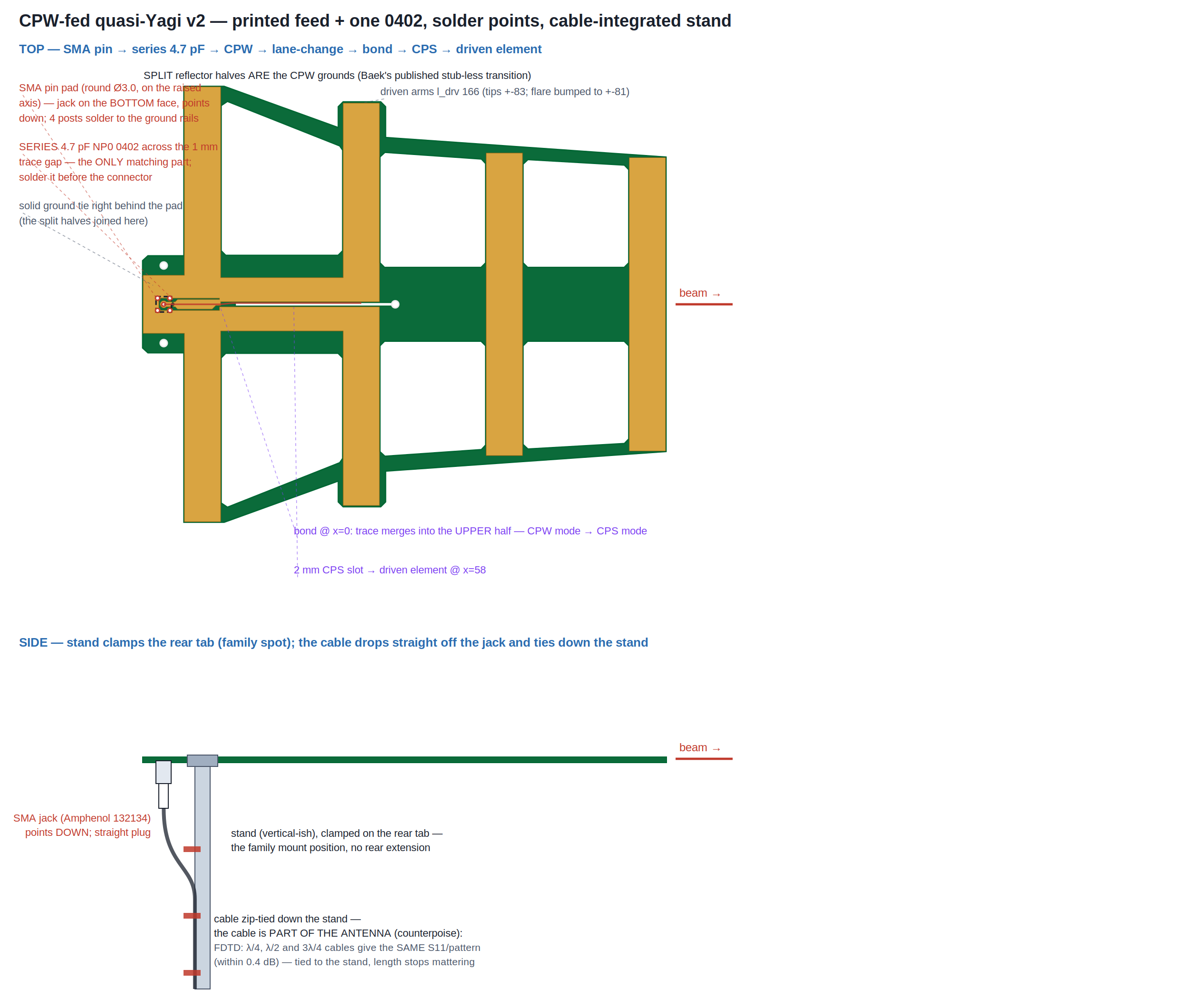
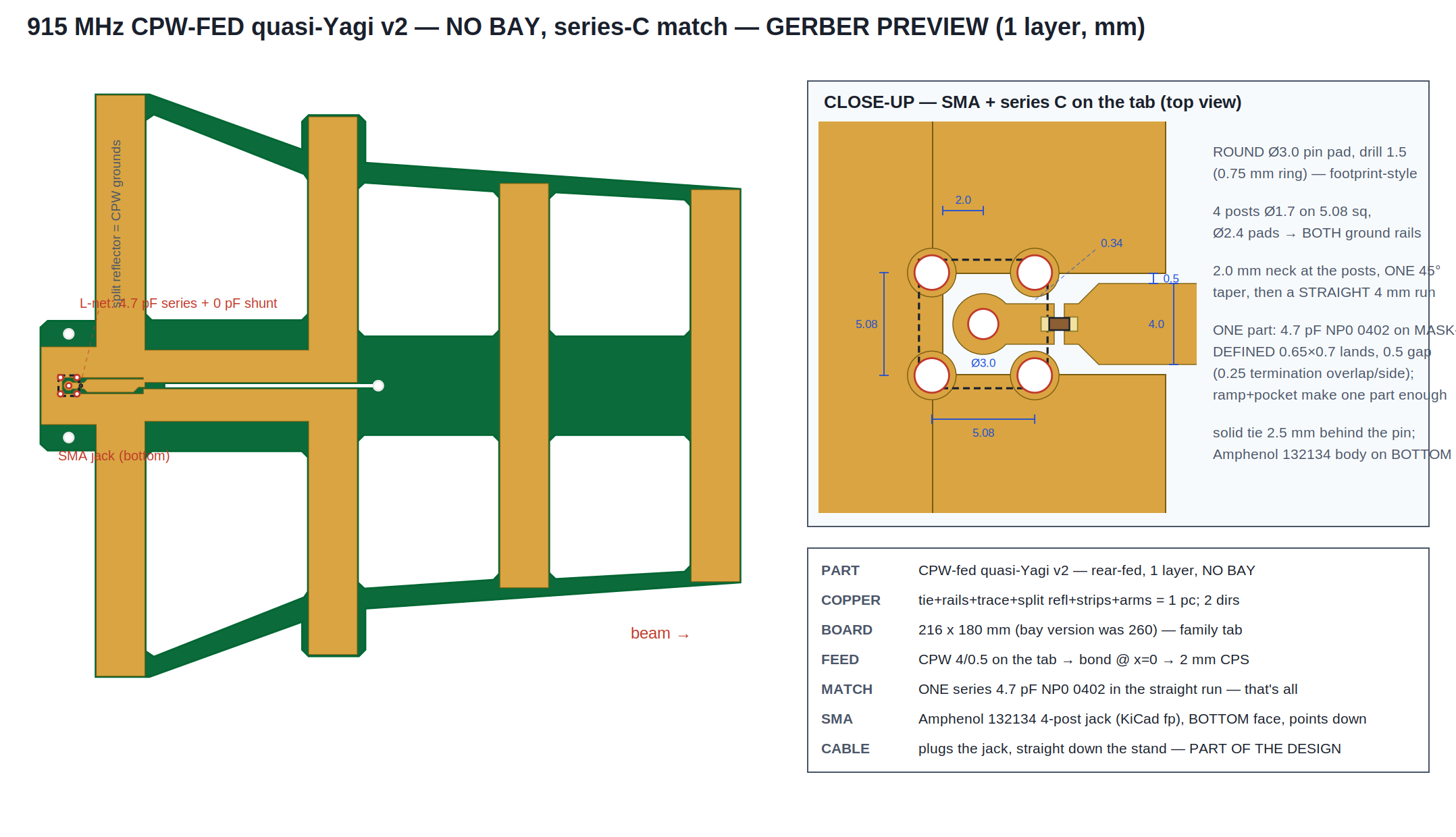
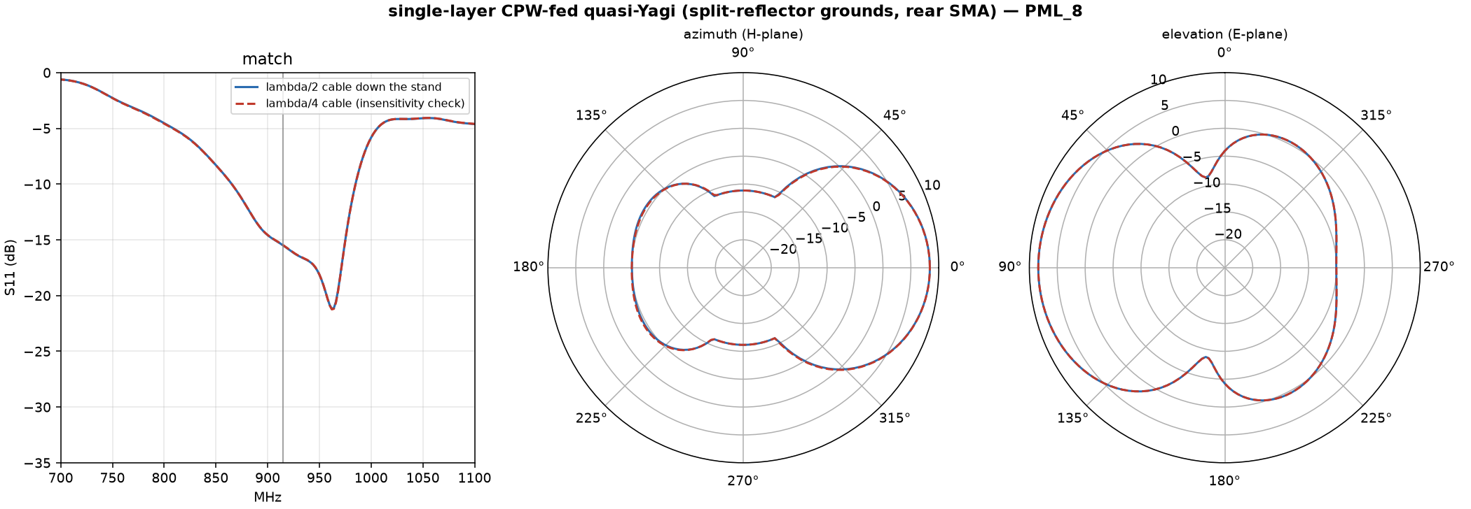
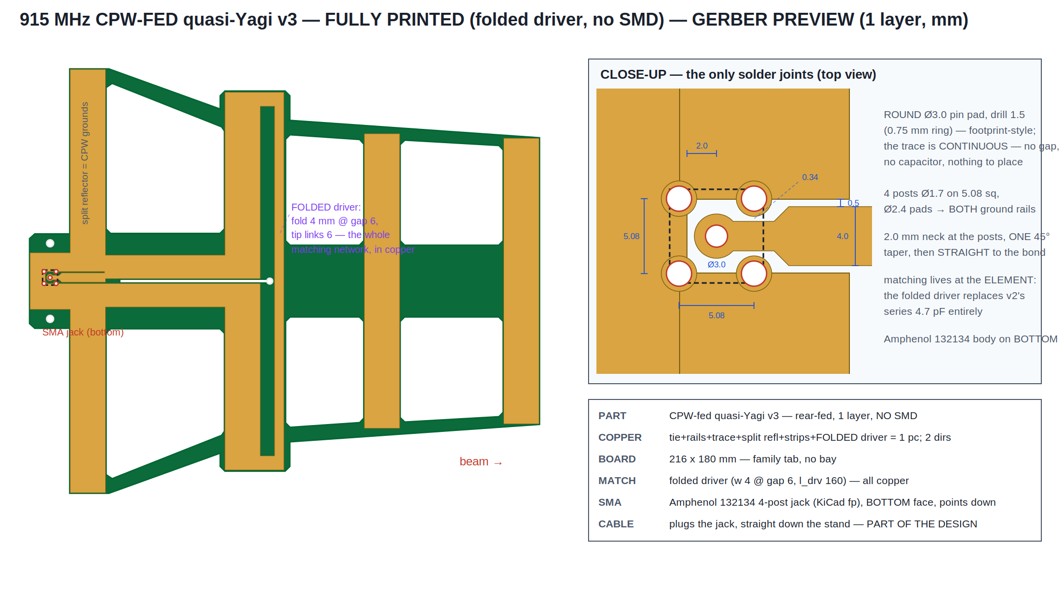
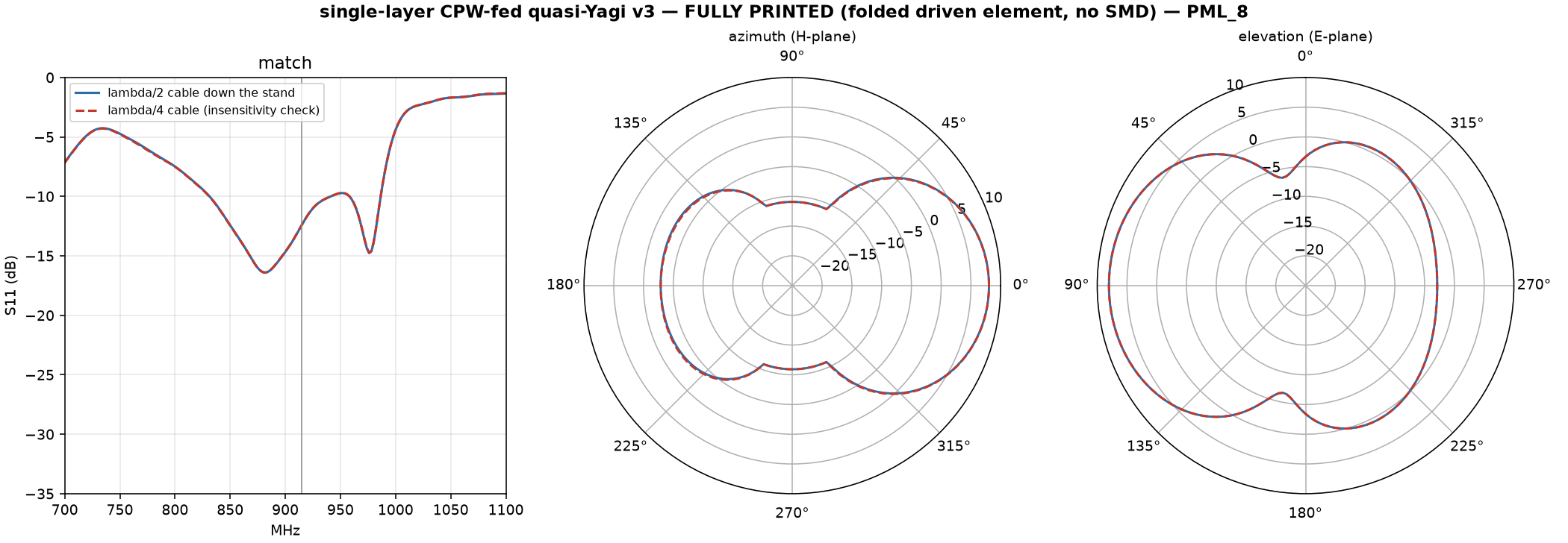
915 MHz · SHIP v2 (no bay, ONE-part match, smooth route) — PML_8 @915 with the λ/2 cable: 8.40 dBi · F/B 13.4 dB · S11 -15.4 dB (Zin 36+3j); λ/4 cable identical: 8.40 / 13.4 / -15.4; MUR rod gate 82/164/246 mm: −16.1/−15.5/−15.6 dB, Zin pinned 42+13j — CABLE-INTEGRATED, the coax down the stand is the designed counterpoise and its length stops mattering · −10 dB band 866–984 MHz · board 216 × 180, FR4 1.6 · THE MATCH IS ONE PART: series 4.7 pF NP0 0402 across a 0.5 mm gap IN THE NECK right at the SMA pad, on MASK-DEFINED 0.65×0.7 mm lands (1005-metric pattern, 0.25 mm termination overlap per side — the manufacturing review caught the old 1.0 mm gap leaving the 1.0 mm part tip-to-tip with zero land; the honest pad geometry costs ~3 dB of match vs that unbuildable layout and is re-verified end-to-end), plus copper only — l_drv 166 is the X-trim, C re-picked 5.6→4.7 for the 0.5-gap fringing (the flare ribs conform to the tips at ±83.5, 0.5 mm routing margin) · SMOOTH ROUTE (three user-driven rounds, every step FDTD-measured): footprint drawn like a pad library — ROUND Ø3.0 pin pad (1.5 drill, 0.75 ring), 2.0 mm neck broken by the C gap, symmetric channel pad, ONE 45° taper to 4 mm, straight run, then a smooth 45° RAMP of the trace's lower edge into the bond (the old right-angle staircase is gone) while the ground edge runs dead straight to the slot mouth — the widening gap between them forms the junction POCKET · WHY THE POCKET STAYS (the negative results that shaped it): raising the whole feed axis +1.5 mm so the lower gap runs straight into the CPS slot looks cleanest but DELETES the pocket — the pad R collapses to ~25 Ω, a single series C saturates at ~−11 dB, and only a two-part L-network (8.2+3.3 pF, measured −27.4 MUR / −18.4 PML) can match it; a parallel ground ramp does the same; the C's position is a one-way street (R falls 36→15 Ω moving pad→bond, so the gap belongs AT the pad — moving it 3 mm downstream during the footprint redesign silently cost 5 dB); tie −26 vs −28 measures IDENTICAL on every new route (the loop-length lever died with the old jog) · v3 — FULLY PRINTED VARIANT (no SMD): folded driven element (fold 4 @ 6 mm gap, tip links 6, l_drv 160, Guertler step-up ≈2.33) on its OWN best-measured route — the RAISED AXIS (+1.5 mm, trace bottom at the transition height, lower gap straight into the slot, no pocket — nothing to feed a C into, and the fold prefers the straight-through): PML_8 λ/2 cable 8.03 dBi · F/B 10.9 · S11 -12.6 dB (Zin 37+16j); λ/4 identical; −10 dB band 832–986 MHz — pick v2 for match depth, v3 for a part-free build · v1 — ALL-PRINTED BAY VARIANT (archived): 58 mm rear extension, PML 7.83 dBi / 11.2 / −9.9, 260 mm board — superseded · CAMPAIGN FAILURE CATALOG (≈100 FDTD runs): (1) bare bond, centered axis — the tie→bond slot ring shunts the bond node (cable counterpoise + matching rescued it); (2) Kan truncated ground — F/B negative; (3) choke slots — never reach λ/4; (4) pure slotline — no balun, cable-dependent; (5) shorted λ/4 slot-tee — series element, blocks the through-path; (6) trace-width λ/4 transformers in the channel — collapse the feed; (7) fold-for-compactness — dead in the reflector's reactive near field (λ/2π ≈ 52 mm), ~15 runs; (8) fully-smoothed feed routes (raised axis / parallel ground ramp) — measured 2-part-only, archived with the L-network numbers; (9) series-C position toward the bond — R falls monotonically, single-element match unreachable there · FAB: real Amphenol 132134 (KiCad footprint) at (−23.5, 0) — footprint-library copper: round pad + in-neck gap + taper (binding clearance = audited 0.34 mm neck-to-post mask web, JLCPCB dam floor ~0.2; CPW gaps 0.5; copper-to-edge 0.2; rings 0.75/0.35); assembly: the 0402 first, then the connector; routed slit tracks the copper slot, crack-stop at its end; zip-ties (−23.5, ±16) · ORDERING (JLCPCB): 2-layer with the provided EMPTY bottom copper; the zips now SHIP THE MASK LAYERS (.gts negative openings only at the solder spots — 0402 lands + SMA rings; .gbs no openings) and an assembly silk (.gto: flange square + 0402 brackets); mask webs ≥0.5 (dam floor ~0.2); HASL, regular ±0.2 outline · OUTDOOR HARDENING (research round): silicone conformal 50–75 µm both faces + routed edges; copper face DOWN; neutral-cure potting at the tab only; brass-SMA torque 0.34–0.56 N·m; FR4 spine for ETSI 300 019 class 4.1; εr corner sweep verified; acceptance S11 ≤ −12 dB over 902–928 clamped on the real stand · gerbonara-validated, shapely DFM-audited (all published JLCPCB floors held)
⬗ stack-up: FR4 1.6 mm (εr 4.3) · 1 oz Cu (35 µm)