Statistical resolution limit (SRL) — closest two targets tellable apart vs SNR · hover a point (session 014z DF model)
Connection detail — Amphenol Connex 132260 + RG-400 jumper
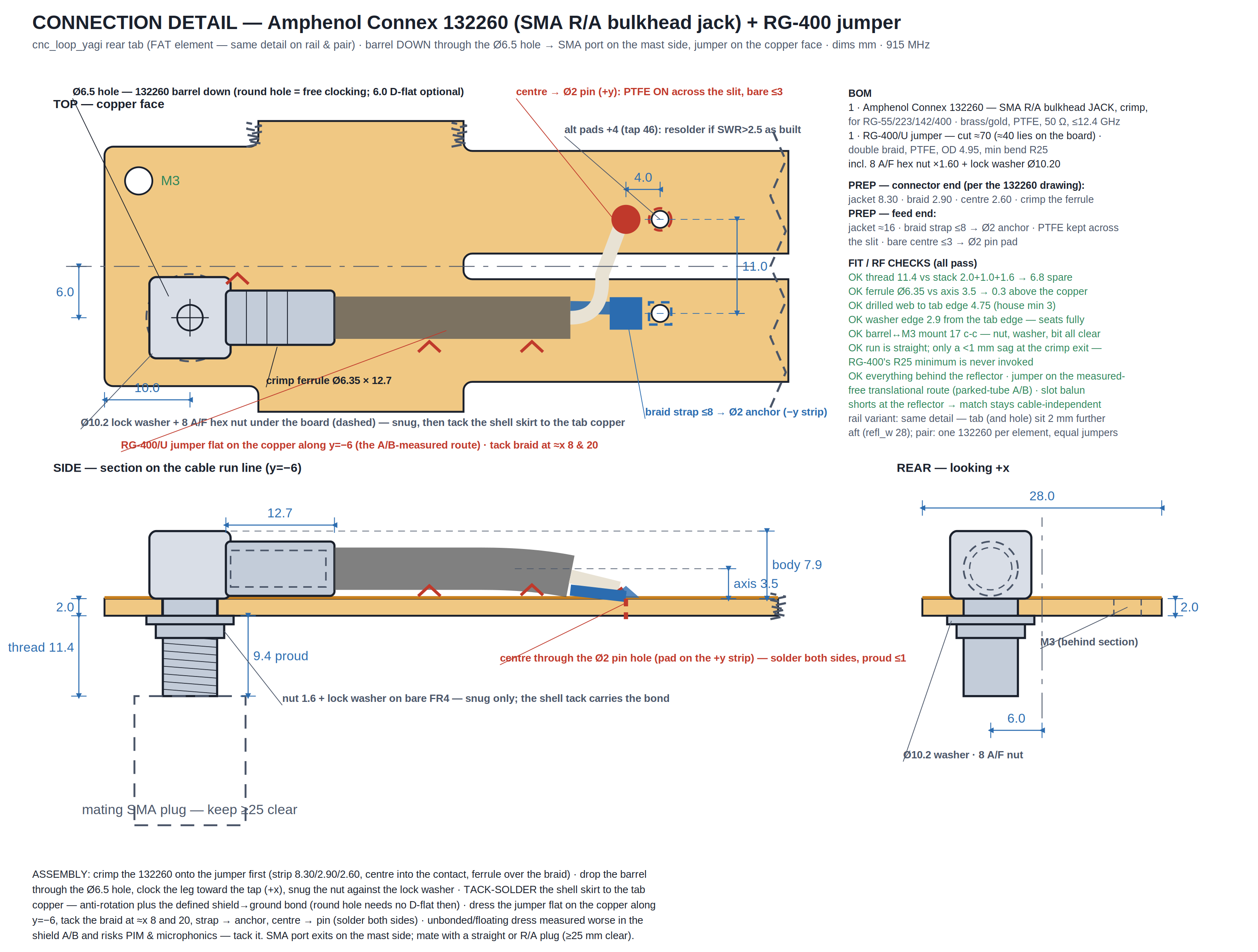
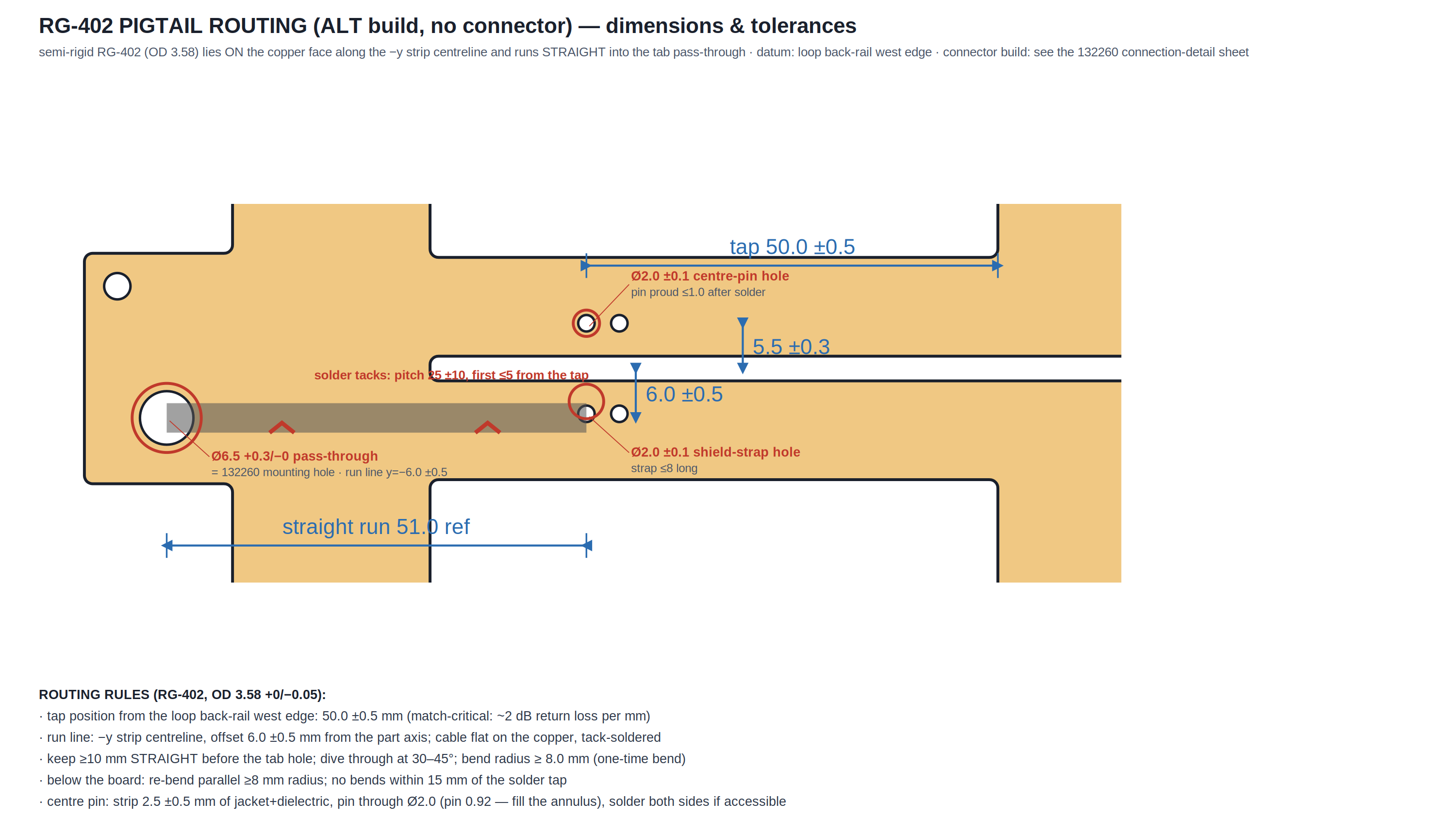
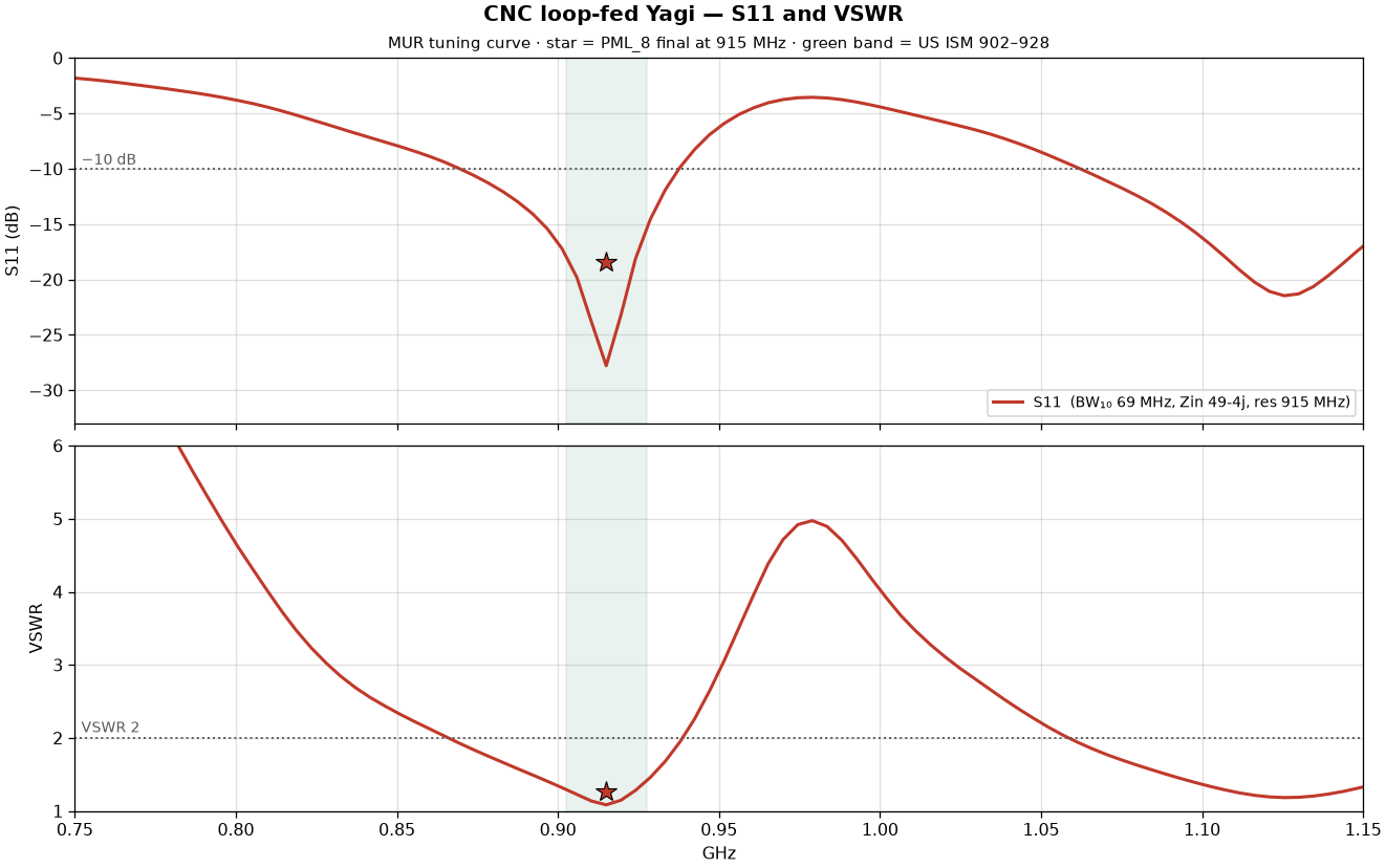
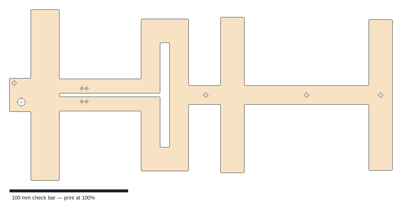
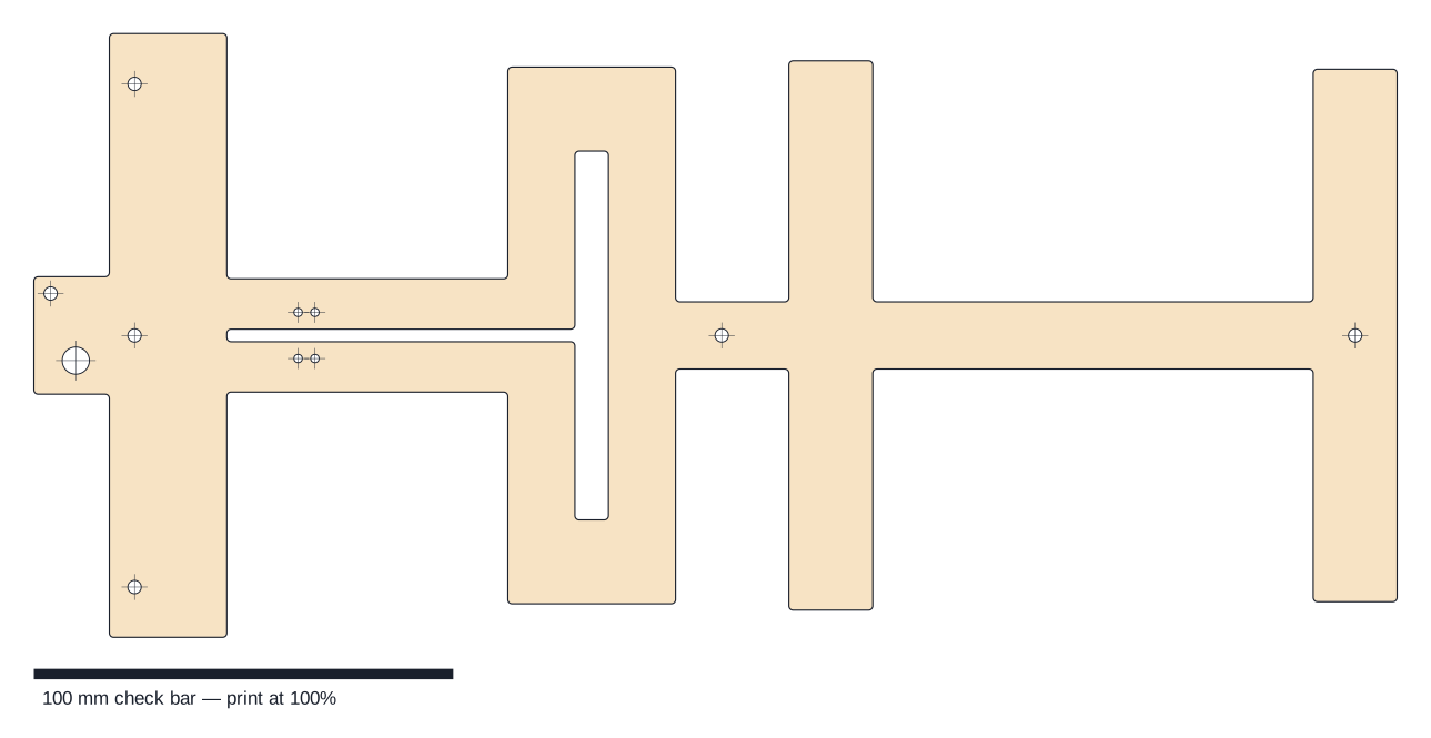
The rear-tab Ø6.5 hole is the 132260's recommended mounting hole (SMA R/A bulkhead crimp jack for RG-400; 1/4-36 barrel, 11.4 mm thread). Barrel drops DOWN through the tab so the SMA port exits on the mast side; the round hole leaves the leg free to clock — point it at the tap, snug the supplied nut against the lock washer on the bare-FR4 underside, then tack-solder the shell skirt to the tab copper (anti-rotation plus a defined shield→ground bond; the 6.0 D-flat becomes optional). The ≈ 55 mm RG-400 jumper lies flat on the copper along y=−6 — exactly the parked-tube route the pigtail A/B measured as ~free, re-measured at RG-400's own Ø5 (not just RG-402's 3.58; full-length tube, mesh-snapped 0.5 mm closer to the slit than the real cable edge = conservative): res lands back on 915.0 exactly, S11 −27.8 → −33.5, BW(−10) 68.6 → 64.0 MHz (still 2.5× the ISM band), D −0.07, F/B +1.0, η −2.0 pts (MUR A/B deltas) — the fat cable is the same ~free class as the thin one, because the slot balun's short does the isolating, not the cable's diameter — braid tacked twice on the way, braid strap to the Ø2 anchor, centre (PTFE kept on across the slit) to the Ø2 pin pad. Fit checks all pass: thread 11.4 vs 4.6 clamp stack (6.8 spare); ferrule Ø6.35 rides 0.3 above the copper; drilled web to the tab edge 4.75 (house min 3); washer edge 2.9 from the edge — seats fully; barrel↔M3 mount 17 c-c; the run is straight so RG-400's R25 bend minimum is never invoked. RF: everything sits behind the reflector, and the slit's short at the reflector (the λ/4 slot balun) keeps the match cable-independent — provided the braid is bonded, which the isolated-shield A/B showed is the part that actually matters. Rail variant: same detail, tab 2 mm further aft; pair: one jack per element with length-matched jumpers.
Rail-mount variant — bolt it anywhere along boom and reflector
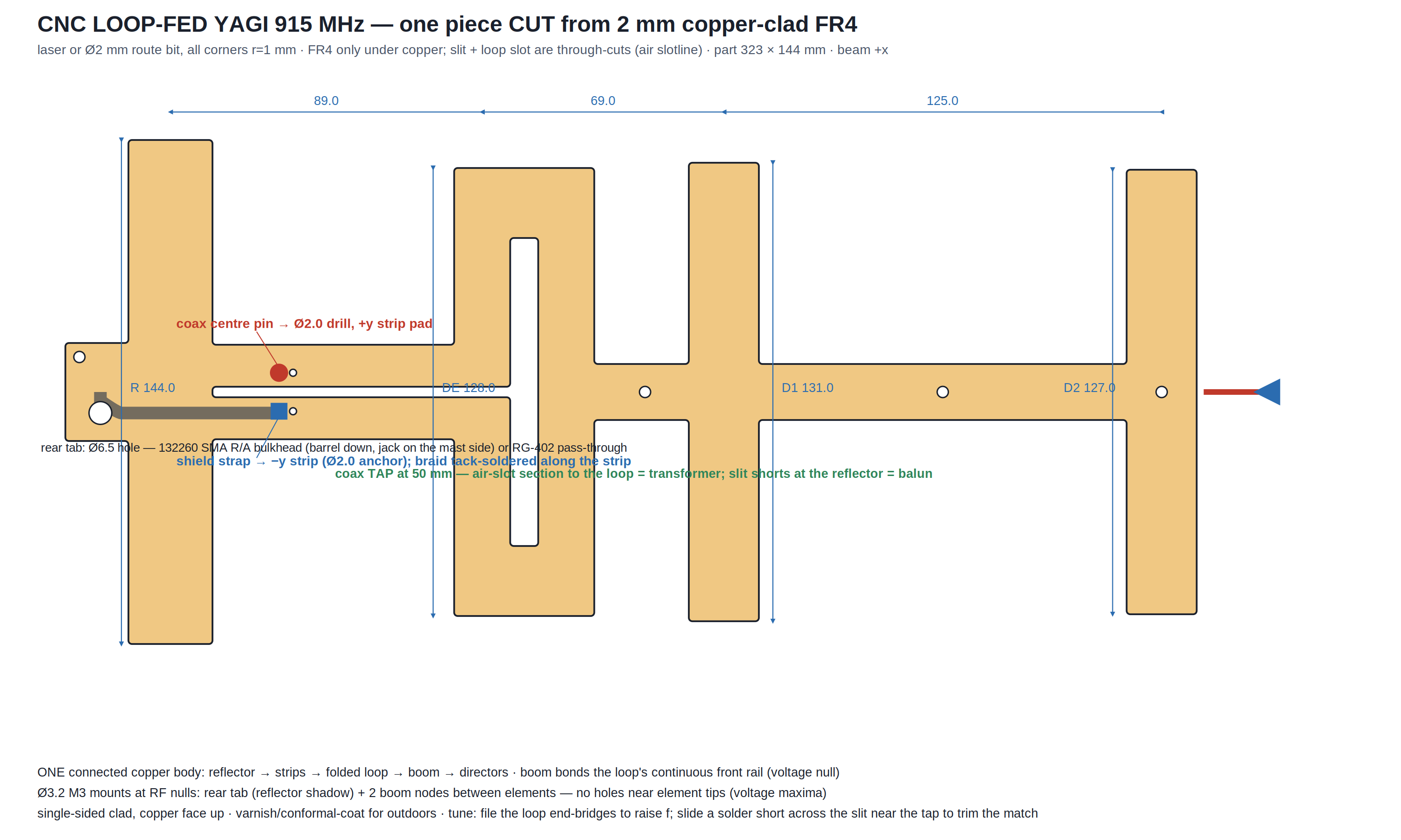
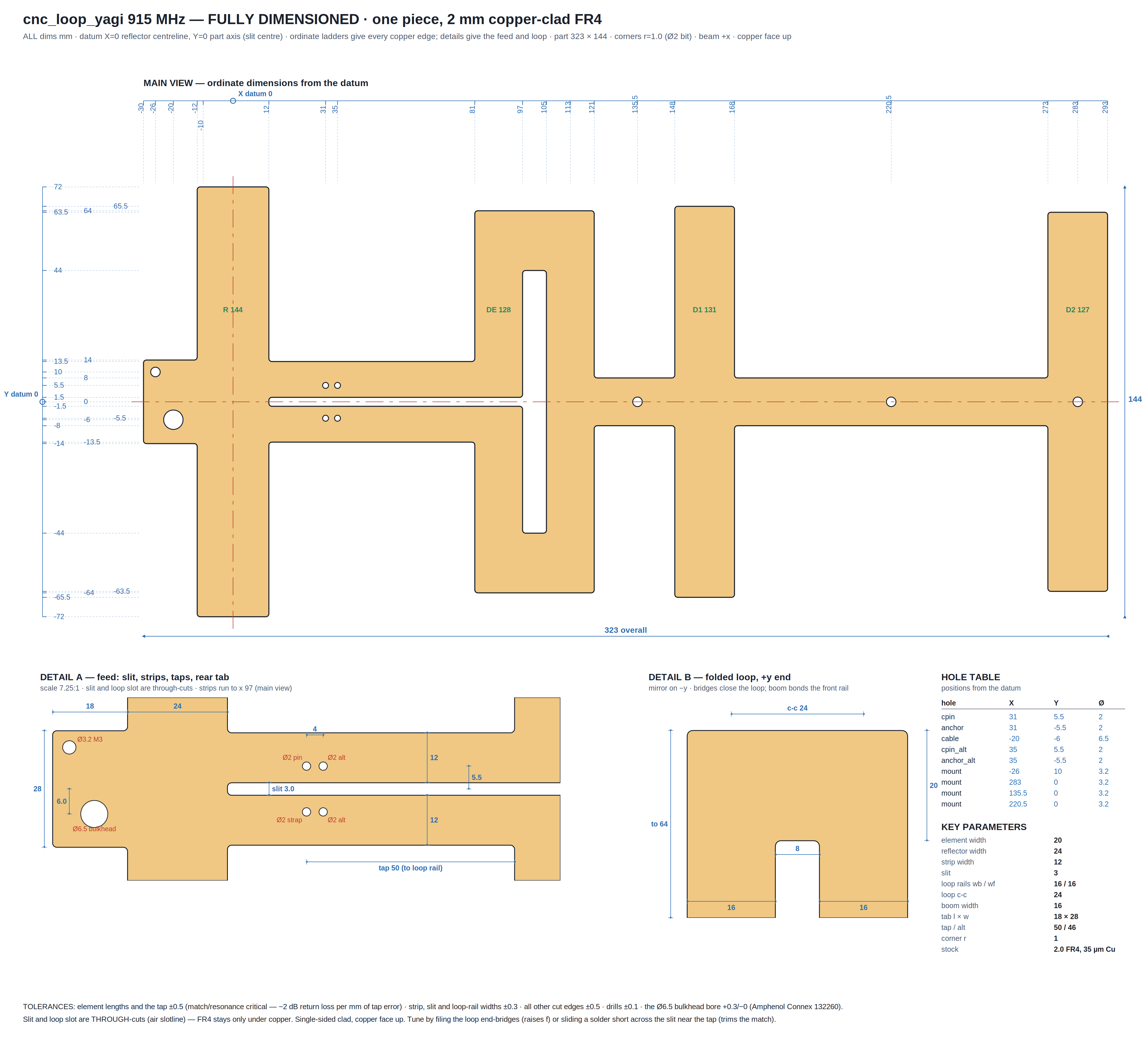
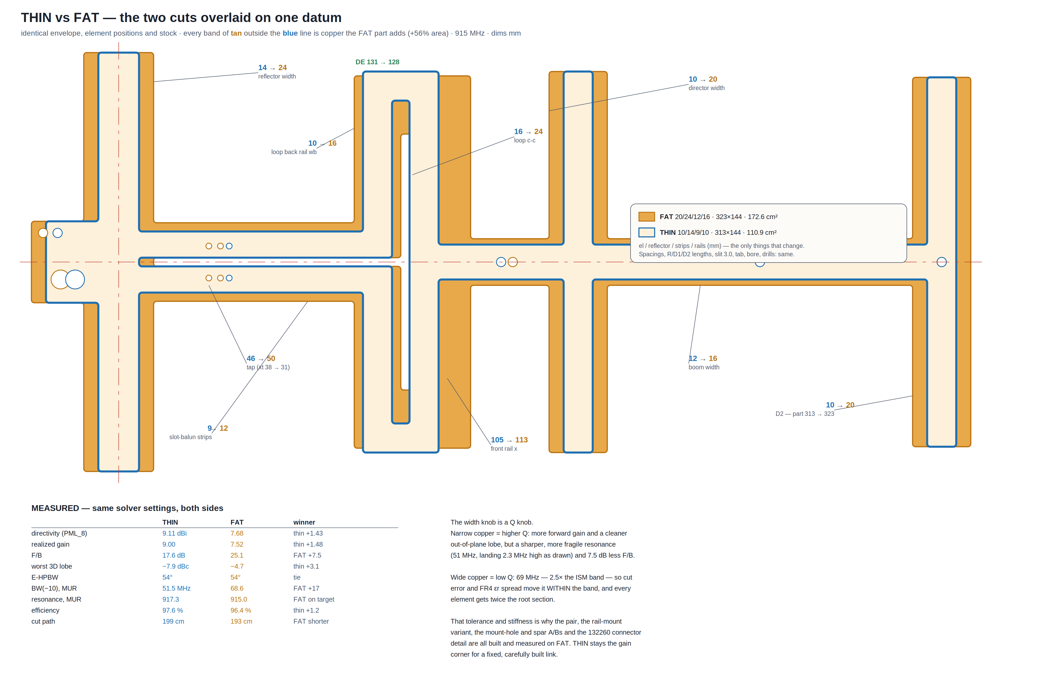
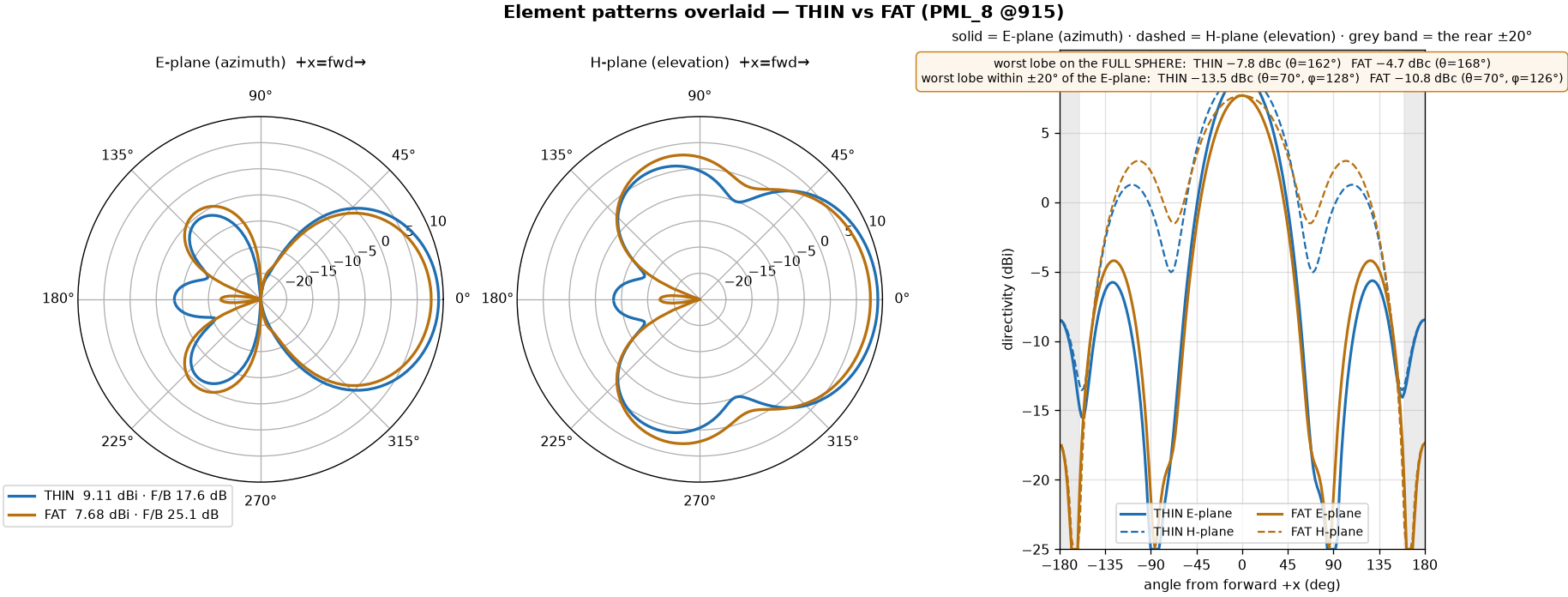
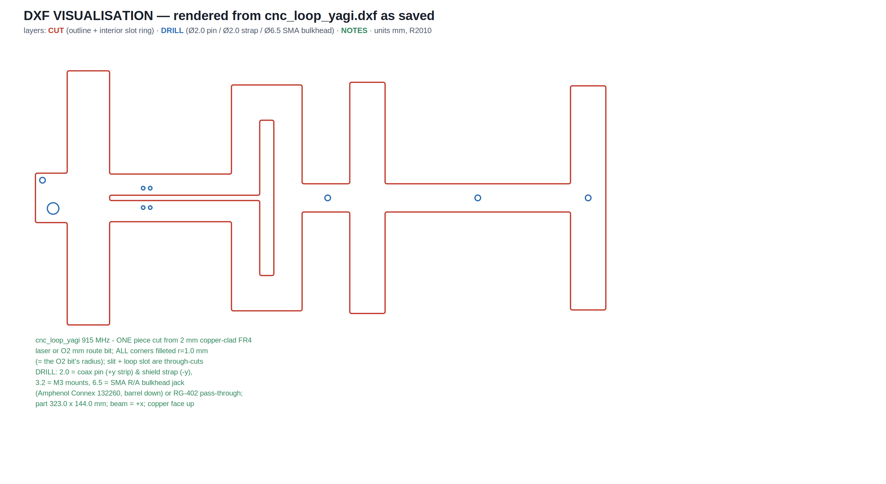
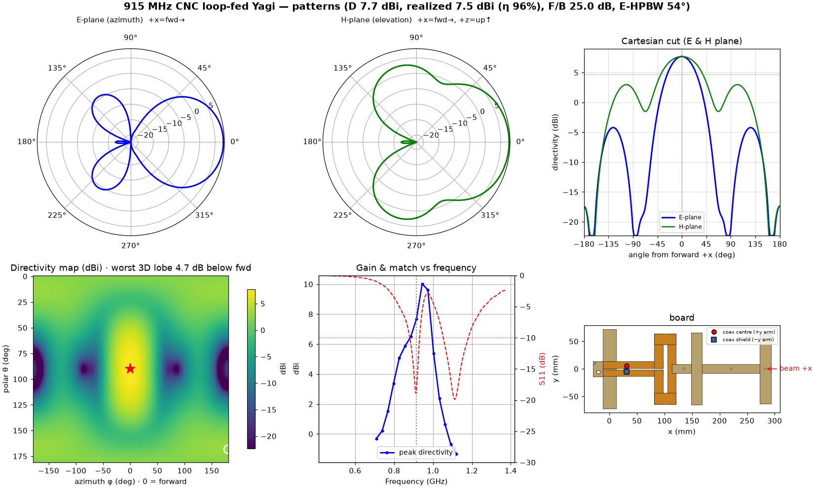
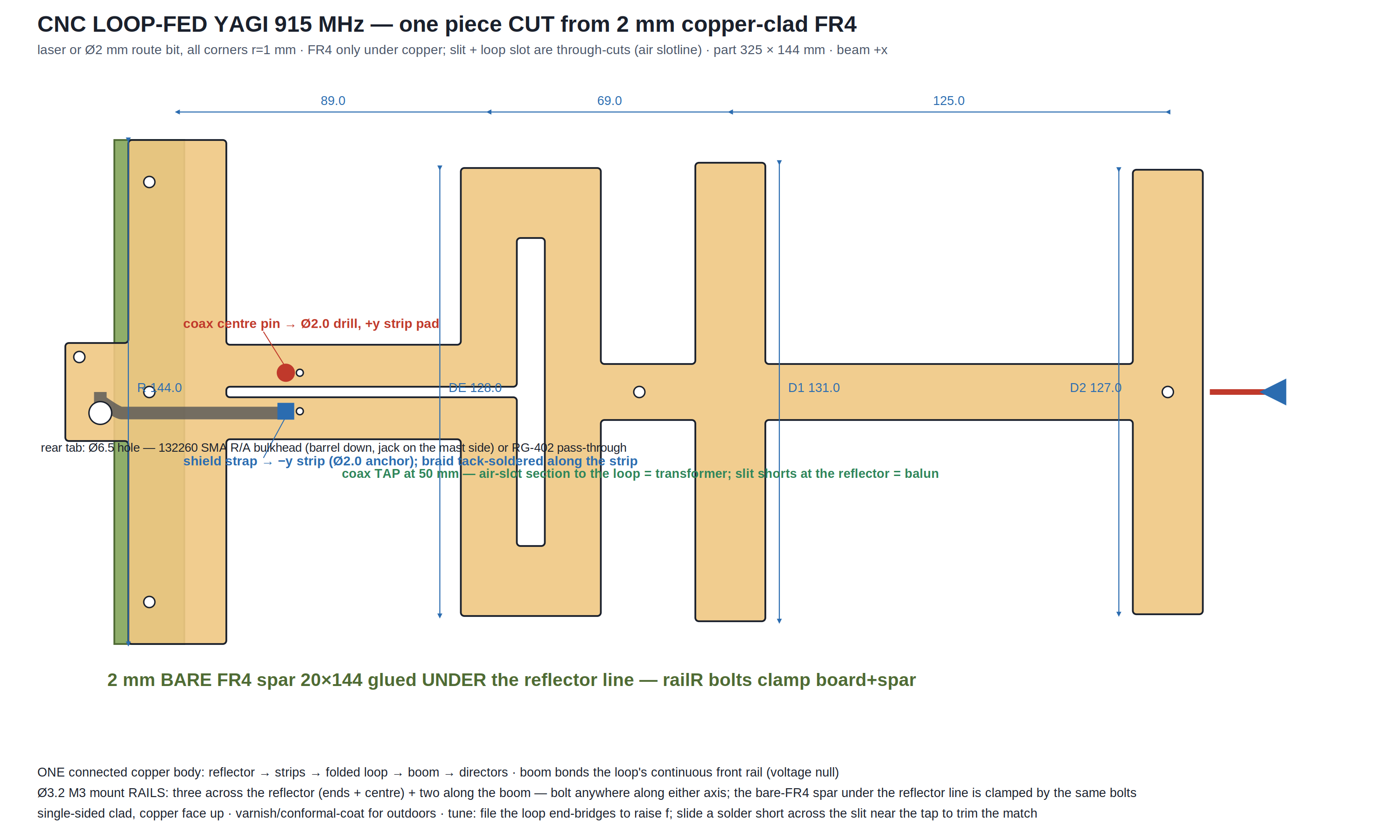
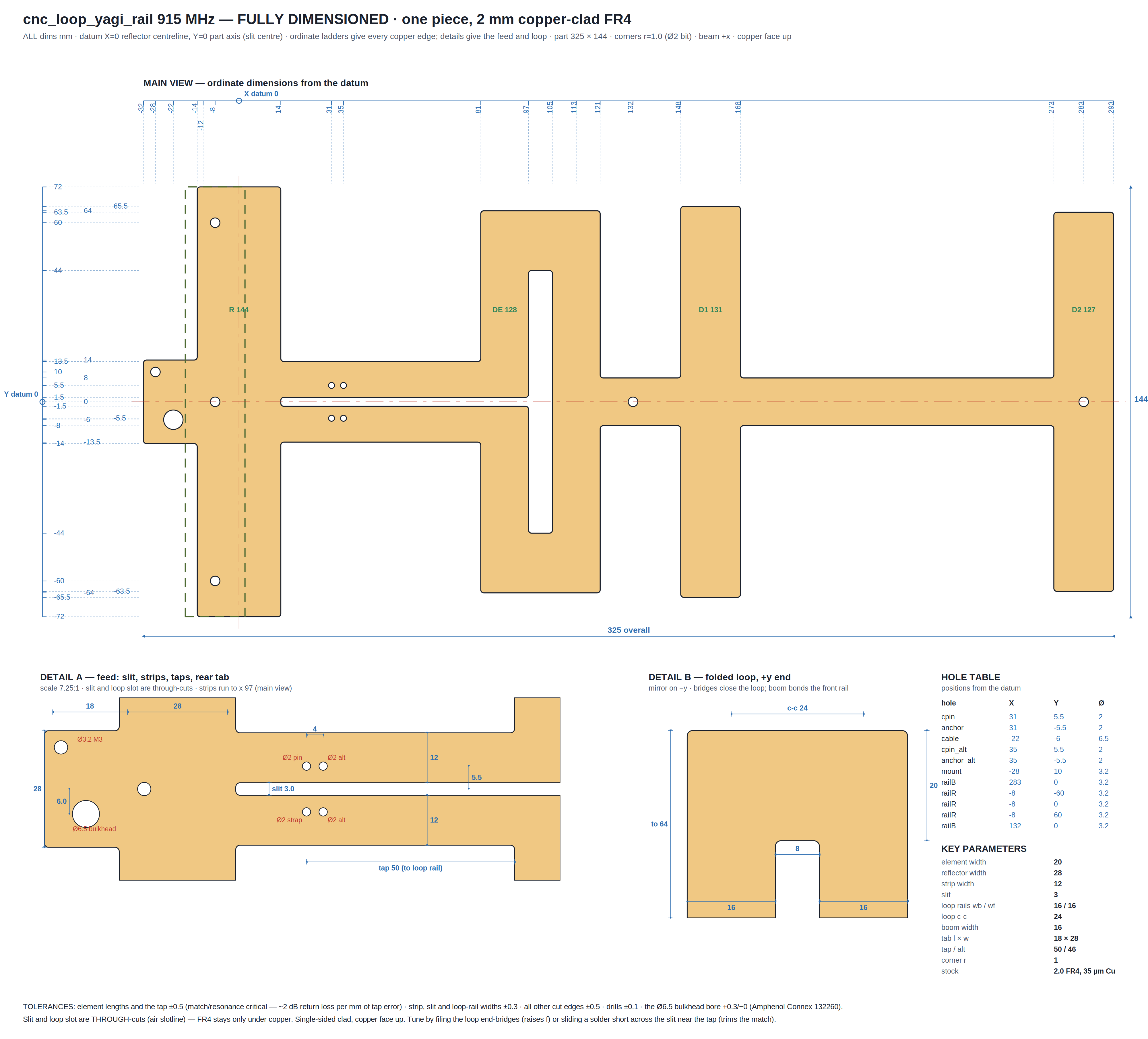
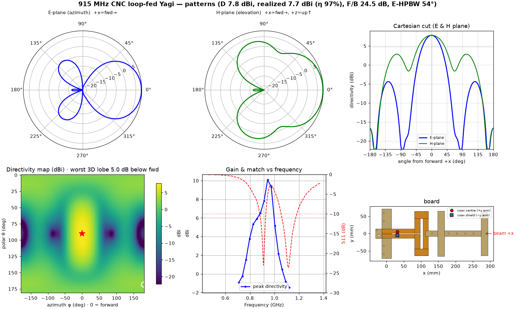
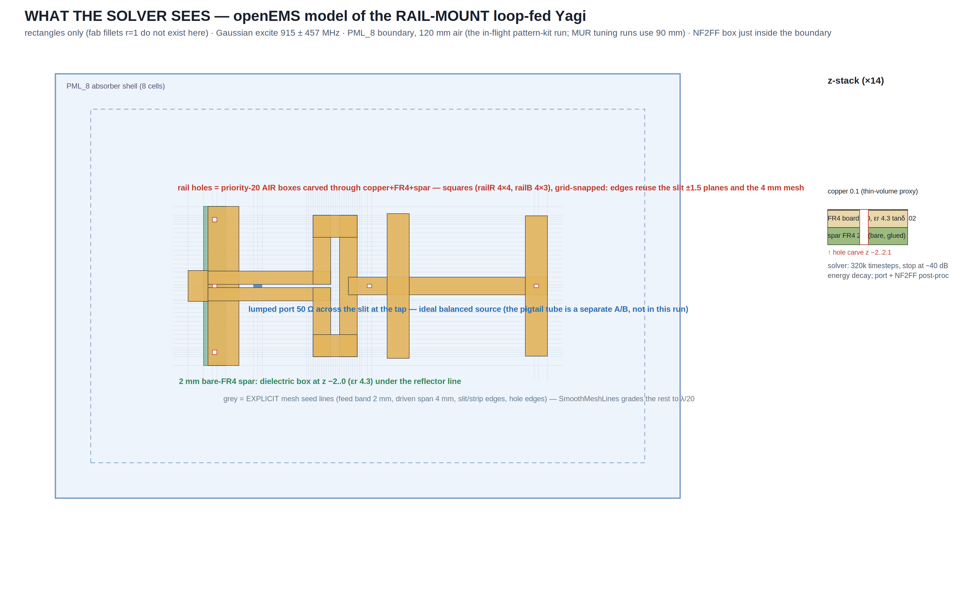
The fat element with Ø3.2 M3 mounts spanning the WHOLE boom and reflector — reflector: three (ends + centre); boom: one at the loop end plus the boom-end hole at the front-director crossing — and a 2 mm bare FR4 spar glued under the reflector line — the pair card's measured-free dielectric bar, here as a mounting spine: the reflector-row bolts clamp board and spar together, so the perforated rear stays stiff and any bolt position along either axis carries the antenna. The reflector row is the RF-sensitive one (it punches the current path), so this variant was SIMULATED, not waved through: holes as grid-snapped cutouts, the row offset to the rear half (rail_xoff −8) so the front copper stays continuous — including the centre hole that sits AT the reflector's y=0 current maximum, which was carved and A/B'd rather than assumed. Measured (MUR, vs the plain fat element): the package is electrically ~free — the spar-only control changes nothing (as the pair found), the full 6-hole row cost 1.1 MHz, and the final 3-hole row none at all (res exactly 915.0, S11 −43.8, F/B 21.3); the boom row rides the voltage-null spine. Reflector width turned out to be a MECHANICAL knob, not an RF one: at the stock 24 mm the hole rims leave a 2.4 mm rear web (below this project's 3 mm no-breakout standard); 28 mm gives 4.4 mm webs for 4 MHz of −10 dB bandwidth (66 MHz, still 2.5× the ISM band) — F/B and gain unchanged, and the match incidentally deepens to −36. At 32 mm a 1.1 GHz mode takes over the S11 minimum: stop at 28. PML_8 finals of the pick: 7.8 dBi (realized 7.7, η 97%), F/B 24.5 dB, E-HPBW 54°, S11 −20.6 (Zin 42−4j), worst 3D lobe −5.0 dBc — all within tenths of the plain element. (The kit was run on the 6-hole predecessor geometry; the final 3-per-axis set was not re-run at PML because the MUR A/Bs bracket it inside run noise — fewer holes, zero resonance shift — and burning an hour of PML to redraw three dots in the layout panel is not honesty, it is theatre.) A boom-end mount sits AT the front-director crossing (the boom bonds dir2 there because it is the director's voltage null; the hole does punch dir2's current maximum, so it was carved into the sim and A/B'd: res unchanged, every metric within run noise — one hole in a 20 mm strip is nothing, consistent with the reflector row). The solver-view figure shows exactly what was modelled: square hole proxies, spar dielectric, ideal port; the DXF carries only the shop part — the spar is a plain scrap rectangle, listed on the NOTES layer with its dimensions and the glue-then-drill-through sequence.
Bench repair tool — for a board that came back at VSWR 3
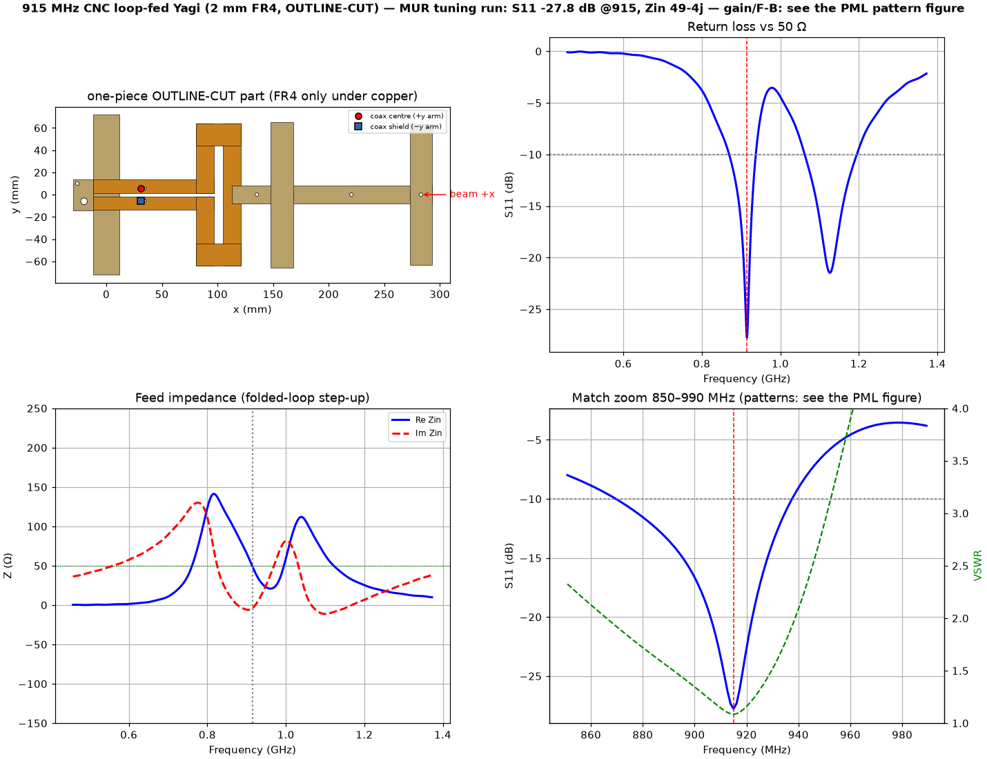
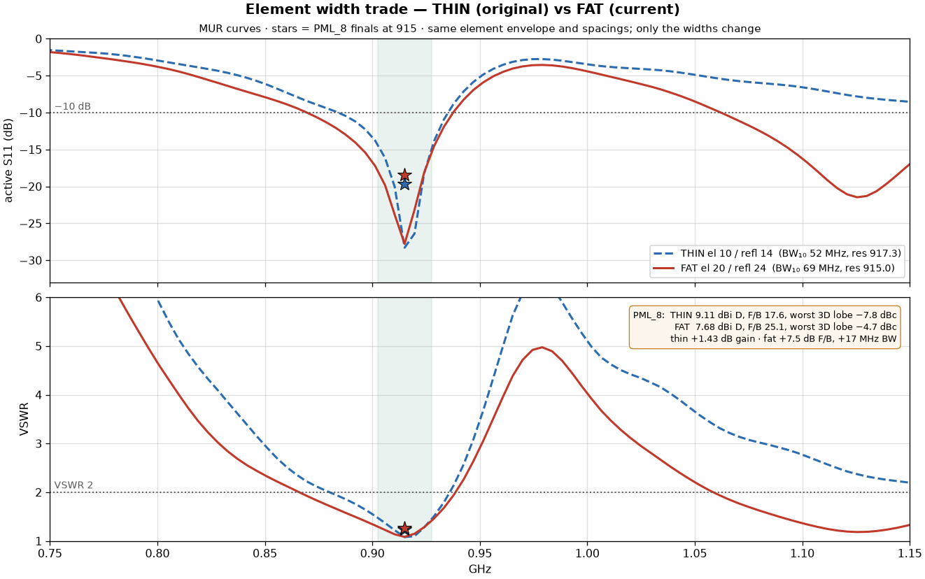
If a cut board measures VSWR ~3 at 915 with its deep dip up near 1117 MHz, the laminate came in at εr ≥ 4.4 and the match crossed to the upper mode — the produced-part failure, reproduced exactly in simulation. It is repairable at the bench with a knife and no change to the outline: scraping a 2 mm band across the director tips shortens them electrically (the detached tip patch stays put, and is modelled that way). Three validated end states, all measured across εr 4.4–4.8 so the recipe never depends on knowing the actual laminate: 2 lines on D1 at 7 mm (VSWR 1.02–1.04, gain 7.3, F/B 19.5), 4 lines on D1+D2 at 5 mm (VSWR 1.09–1.13, gain 8.5, F/B 25–26), or 6 lines adding the reflector at 4 mm (VSWR 1.28–1.34, gain 9.1, F/B 42–46). Measured dead ends worth knowing: the reflector pair alone changes nothing (VSWR stays 3.5), D2 alone changes nothing, scraping the loop bridges is worse, and a single asymmetric line works but sits 2 mm from a cliff where the mode flips back — so two lines is the honest minimum. The downloadable tool (cnc_loop_scratch_app.html — open it in a browser, no install) takes the two VNA numbers, confirms whether this is that fault or something else entirely, draws the cut positions on the real outline with a magnified tip detail, and checks the re-measurement against the chosen recipe's window.